HP of Ohoyama Lab.
Local atomic Structure of functional materials using holography
Most of functional materials, the properties can be controlled by doping small aount of foreign elements. Typical case is Si semiconductor, in which very small amount of B or P is deped to change the performance as a semiconductor. We are investigating the effeects of doping to atomic structure and properites by observation of local atomic structures of light elements, such as B, O, H.
Neutron scattering is a powerful prove for structural physics, in particular, observations of light elements. For most of neutron scattering techniques, the data are obtained in Q-space, meaning that the periodicity in materials is the target. However, in many functional materials, atomic structures without translation symmetry in lattices play important roles. For instance, the properties of Si semiconductor can be controlled by B or P doping with a concentration of 10-3-10-7 %. Thus, from a view point of structural physics, it is highly probable that slight distortion of atomic structures around the dopant must be important to understand the functionalities. The distorted atomic structures around dopants is called local structures. For investigations of local structures, the powerful probe is atomic resolution holography, which has the following advantages.
1: Local atomic structures around selected elements (dopants) can be visulaised.
2: 3 dimensional (3D) local atomic structures can be directly obtained without structure models.
3: The observable range is ~20A, which is larger than typical lattice constants of inorganic materials.
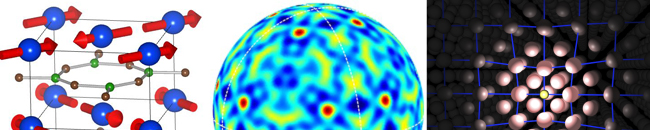
Atomic resolution holography by electrons and radiation x-rays have already provided rich and novel results of local structures. In 2017, we succeeded in developing world-first white neutron holography in Japan Proton Accelerator Research Complex (J-PARC) at Tokai, Japan)[1,2]. For white neutron holography in J-PARC, one can obtain data (holograms) with ~130 different wavelengths in the range of 0.36A - 6.5A at once. This is the essential point to enhance accuracy of atomic images drastically.
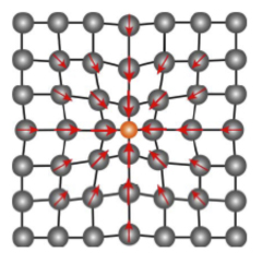
We successfully visualised local atomic structures around Eu in 1% Eu doped CaF2, and found that there exist excess F- around Eu3+ dopants. We have visualised local atomic structures in many materials in J-PARC already: the semiconductor 0.26% B doped Si[2], the thermoelectric material 0.75% B doped Mg2Si, the typical strongly correlated electrons system 2% Sm doped RB6 (R: Yb, La), and so on. Fig.1 shows local atomic structure around 10B (green) in 0.26 % 10B doped Si2). The Si structure around doped 10B is the diamond type, directly indicating that most of 10B are located at Si positions in spite of higher concentration. Fig.2 shows atomic images of Yb around Sm (green) in 2% Sm doped Yb11B6 (space group:Pm-3m, a = 4.16 A). We also visualised B cages around rare earth atoms. At least 7th nearest neighbour Yb located at 12.5A from Sm was visualised. We found the suppression of intensity of the atomic image of 1st NN B around Sm, while those of more distant B and R are consistent with the calculation by a non-distorted model, indicating that the only 1st NN B is fluctuated by Sm doping while other B and R are stable at the non-distorted position because of strong valence bonding of B-cages. These results indicate that white neutron holography is a strong probe for observation of doping effects and determination of the dopant positions in materials with light elements.
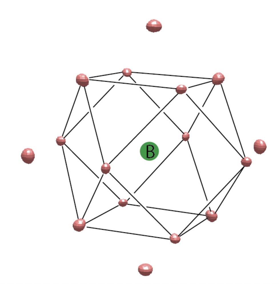 Fig.1 Local Atomic Structure of Si around B in 0.26at% B doped Si[2] |
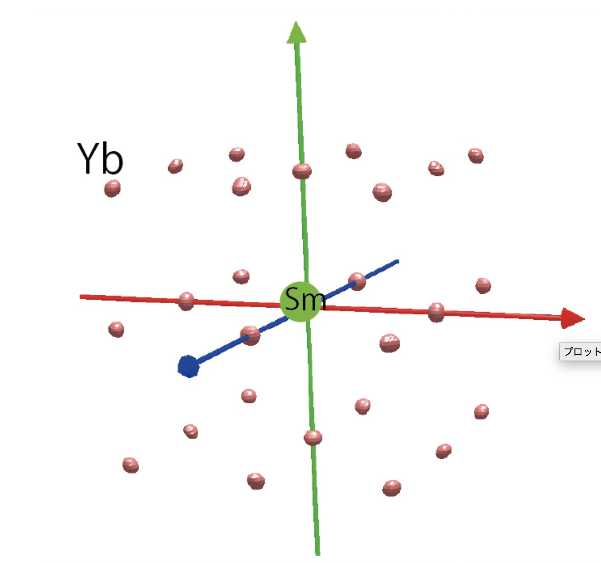 Fig.2 Local Atomic Structure of Yb around Sm in 2% Sm doped YbB6 |
References
[1] Hayashi, Ohoyama et al. Sci. Adv., 3 (2017) e1700294.
[2] Ohoyama and Hayashi, Phys. Status Solidi B 255(2018) 1800143
[3] Hayashi et al, AIP Advances 10, 035115 (2020)
Materials which were succecefully visualised using white neutron holography
We succeeded in visualising local atomic structure around dopants of the following materials.| Dopant | Concentration | Maerials | Ref | |
| B | 0.13, 0.26at% | Si | Semiconductor | [2] |
| Sm | 2 % | LaB6 | Strongly Correlated Elctrons System | |
| Tm | 2 % | YbB6 | Strongly Correlated Elctrons System | |
| B | 0.06 % | SiC | White LED | |
| B | 0.7 % | Mg2Si | ThermalElectric Material | [3] |
| Eu | 1% | CaF2 | Scintilation crystal | [1] |
What you can do using white neutron holography?
1: You can determine dopants positions in the lattice by visualisation of local atomic structures around the dopants.
2: You can also observe doping effects to the lattices of materials, in particular fluctuations by the doping.
3: You can estimate amounts of dopants located at the substitutional and interstitial positions.
